Announced: 16 June 2020
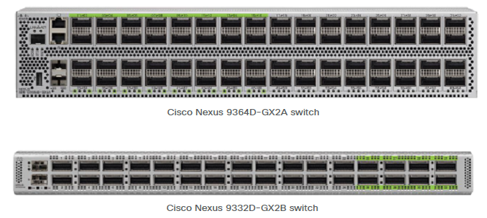
The datasheet has some challenges. At the top, it lists the number of slice-pairs. I am imagining that this is the combination of an input slice and an output slice. If that is true then 30 MB (1/4th of 120 MB) for the GX2A will be divided between output and input buffering. Usually the output buffer gets the larger share. So max burst absorption will be something less than 30 MB. And for the GX2B, it will be half of 120 MB -- or something less than 60 MB.
As noted in the blog post, the feature geometry of these ASICs is 7 nm. These switches have not yet been featured in a CiscoLive! presentation. That can change at any time.
Noted in the Announcement, the GX2 uses multi-die technology, i.e. chiplets. There are advantages and disadvantages to chiplets over a single integrated silicon ASIC. Power consumption is higher with chiplet implementations.
The GX2 ASIC is also used in a 16-port 400G line card for the Nexus 9500 chassis.